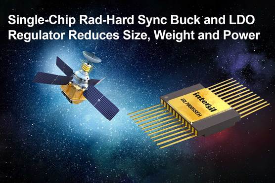
Monolithically Integrated ISL70005SEH Space-Grade Power Solution Reduces BOM Count and Size, Weight and Power for FPGAs and DDR Memory
Renesas Electronics Corporation (TSE:6723), a premier supplier of advanced semiconductor solutions, today announced the industry’s first single-chip synchronous buck and low dropout (LDO) regulator targeting low-power FPGAs, DDR memory and other digital loads for spaceflight payload applications. The ISL70005SEH is the only point-of-load (POL) power solution that reduces size, weight, and power (SWaP) by integrating a synch buck and LDO in one monolithic IC. The device enables satellite manufacturers to reduce bill of materials (BOM) and power supply footprint for their medium Earth orbit (MEO) and geosynchronous Earth orbit (GEO) long duration mission profiles.
The ISL70005SEH rad-hard dual output POL regulator combines 95 percent high efficiency with the synch buck regulator and a low 75mV dropout on the LDO regulator. The device enables easier thermal management for systems with 3.3V or 5V power buses and can support 3A continuous output load current for the buck regulator and ±1A for the LDO. The buck regulator uses a voltage mode control architecture and switches at a resistor adjustable frequency of 100kHz to 1MHz, enabling a smaller filter size.
“The ISL70005SEH gives satellite manufacturers the superior radiation performance, and SWaP and BOM savings they want,” said Philip Chesley, Vice President, Industrial and Communications Business Division at Renesas. “Our dual output POL regulator also provides the configurability to address multiple applications in commercial telecommunication satellites, military satcom satellites, and science and exploration missions.”
The space-grade ISL70005SEH simplifies design configuration allowing designers to use it as a dual output regulator, DDR memory power solution or high efficiency low noise regulator for RF applications. The flexible LDO can source and sink current and accept input voltages as low as 775mV to reduce unnecessary power dissipation. The externally adjustable loop compensation on the buck allows users to achieve an optimal balance of stability and output dynamic performance. The device is wafer acceptance tested to 100krad(Si) over high dose rate (HDR) and tested for ELDRS up to 75krad(Si) over low dose rate (LDR). Single event effects (SEE) testing shows no single event latch-up (SEL) and single event burnout (SEB) at a linear energy transfer (LET) up to 86MeV∗cm2/mg. Single event transients (SETs) have been characterized at a LET range of 8.5 to 86MeV∗cm2/mg.
Key Features of ISL70005SEH Dual Output POL Regulator
- Synchronous buck Vin range of 3V to 5.5V
- LDO Vin range of 600mV + VDO to Vcc-1.5V
- 1% reference voltage accuracy
- Separate VIN, enable, soft-start and power good indicator
- LDO stable with 150µF; 3x less output capacitance than competitive solutions
- Full military temperature range of -55°C to +150°C
The ISL70005SEH is a single-chip power solution for both FPGA core and I/O rails and can be combined with Renesas analog signal chain ICs to create a satellite telemetry solution: ISL70444SEH 40V quad operational amplifier, ISL71840SEH 30V 16-channel multiplexer, ISL70591SEH 100µA precision current source and ISL71090SEH12 1.25V precision voltage reference.
The ISL70005SEH also combines with other Renesas power management ICs to form a complete power solution including redundancy, protection and sequencing for high processing FPGAs: ISL70061SEH 10A PMOS load switch, ISL70321SEH quad power supply sequencer, ISL75051ASEH 3A LDO, and ISL70003ASEH 9A buck regulator.
Availability
The ISL70005SEH radiation-hardened dual output POL regulator is available now in a 28-lead ceramic dual flatpack package or in die form. An evaluation board is available to evaluate device features and performance. For more information, please visit: www.renesas.com/products/ISL70005SEH.


