Terry Lo, Automotive Power Systems Engineering Manager
Fil Paulo Balat, Applications Development Manager
Siglo Raphael Alcantara, Applications Development Engineer, and
Michael Lacson, Senior Applications Development Engineer
Abstract
A quad output, triple monolithic buck converter and boost controller reference design is presented that applies to automotive electronics such as a telematics box. The reference design features a fault protection scheme to support against input transients such as load dump, cold crank, or reverse battery.
Introduction
Voltage transients from the energy generated by the car alternator and ignition system, or fault events due to external factors such as a car crash, can affect the electronic circuitry in an automotive system. Reliability of the electronic circuitry may be greatly affected; therefore, protection against these unpredictable events must be considered. A telematics box, for example, is an electronic system inside the car that requires high reliability and protection.
The power system design in this article is a reference design solution to provide protection and reliability to a car electronic module that requires four voltage inputs. It features input fault protection against load dump, cold crank, and reverse battery. A PowerPath™ controller allows smooth switch-over between the main and backup batteries when input fault protection is active. A quad output regulator provides four voltage outputs with a triple monolithic buck converter and a boost controller. One of the buck outputs can be made to handle high output peak current requirements, such as those on a communication module. There is a provision for charging the backup battery through a linear battery charger when the main battery is active. Figures 1 and 2 show the basic block diagram and the evaluation board of the reference design solution.

Figure 1. Basic block diagram of the reference design.

Figure 2. Evaluation board hardware.
Fault Events and Scenarios
Load Dump
Load dump occurs when the alternator system is charging a battery and the connection to the battery is lost. A battery may be disconnected because of cable degradation, improper connection, or purposeful separation while the engine is running, resulting in a load dump. Alternator systems without centralized load dump suppression allow the alternator to produce extremely high voltages in the event of a sudden battery disconnection. The voltage dumped onto the load can go up to 100 V for a 12 V system due to the stator’s high inductance and the vehicle’s voltage regulator’s inability to reduce the field current rapidly enough.

Figure 3. A load dump scenario.
Cold Crank
During startup or cranking, the engine requires more power, causing the battery voltage to dip. In general, starting an engine in a cold environment is harder than starting an engine in a warm environment. This requires the engine to draw more power, which results in a larger voltage drop compared to normal cranking. This condition is known as cold crank. The waveform in Figure 4 shows the waveform during cold crank where the main battery falls below its specified level.

Figure 4. A sample cold crank scenario.
Reverse Voltage
A reverse voltage or, simply, reverse battery condition covers the human error scenario where someone connects a battery with the polarity reversed. This can result in destruction unless adequate protection is provided.
Circuit Function
Fault Protection
The LTC4367 serves as a fault protection for the circuit as it disconnects the VBATT voltage to VIN when the VBATT voltage is too low, too high, or negative. It has accurate overvoltage and undervoltage comparators to ensure that power is applied to the system only if the input supply is within the allowable voltage window. The LTC4367 automatically isolates the load from negative input voltages. It can operate an overvoltage protection that can go as high as 100 V and undervoltage protection that can go as low as –40 V.

Figure 5. Block diagram of a typical circuit and its function.

Figure 6. VBATT valid and fault protection window.
Backup Battery
Backup battery charging is possible through the LTC4079, which features a multichemistry battery charger that allows a flexible battery voltage to be used. With the reference design circuit, a charging voltage of around 4.2 V is used. To avoid overcharging the battery, the LTC4079 also features a charge termination capability through a C/10 detector or a set charge timer of around 2 hours and 30 minutes.
Automatic switch-over between VBATT and VBACKUP is possible through the LTC4412 PowerPath controller. This feature allows the LT8603 to maintain an output voltage on VOUT4 by having a VIN drawing from either VBATT or VBACKUP. In the event of VBATT disconnection or fault detected, the controller allows the current to flow from the VBACKUP to the VIN of the LT8603. When no fault is detected, the LTC4412 will block the path connecting the VBACKUP to the VIN of the LT8603. Figure 7 shows the waveform of the power switch-over event.

Figure 7. Power switch-over event at cold crank.
In the event of a cold crank, VBATT goes down from 12 V to 2 V. The VBATT path is disconnected, and VBACKUP now serves as the VIN of the boost converter in order to maintain an 8 V output on VOUT4. When VBATT increases to ~5 V, it will again serve as the VIN for the boost converter. VOUT4 will still be maintained at 8 V until VBATT reaches 8 V. As VBATT recovers to its original voltage of 12 V, VOUT4 will then follow the voltage of VBATT. A small voltage drop on VOUT4 is due to the diode forward voltage. The power switch-over allows VOUT1, VOUT2, and VOUT3 to maintain its regulation.
Quad Output Regulator
The LT8603 features a boost regulator, VOUT4, with two high voltage buck regulators, VOUT1 and VOUT2, and a low voltage buck regulator, VOUT3. The boost regulator is capable of providing power to the buck regulators. The LT8603 provides good input and output load regulation at different input voltage levels. Figure 8 shows the output regulation of the LT8603.

Figure 8. Output regulation of the LT8603.
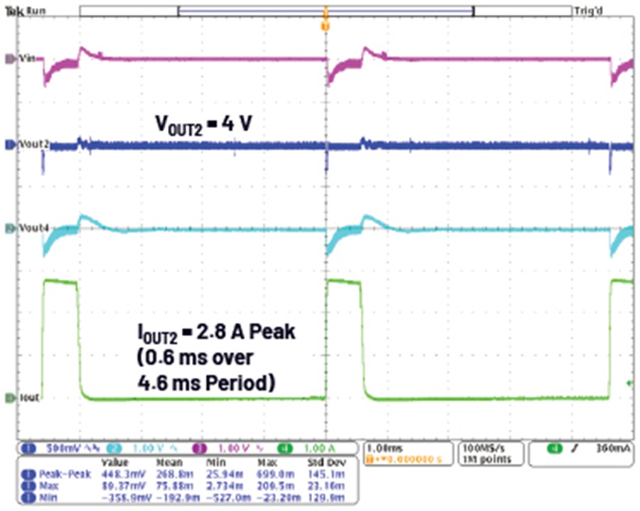
The high output peak current capability of one of the buck regulator outputs, VOUT2, of the LT8603 is used for applications that involve a communication module. A typical 3.6 V to 4 V output voltage and an output peak current on-time of 0.6 ms over a 4.6 ms period is required for a communication module. On the tested conditions shown in Figure 9, the system’s transient behavior is monitored. VOUT2 features a good transient response with minimal voltage undershoot and overshoot.

Figure 9. High output peak current performance of VOUT2.
Load Dump Response
The input fault protection and power switch-over feature of the reference design board allows the LT8603 to operate despite being in a load dump event. Figure 10 shows a simulated waveform of a load dump condition where VBATT goes as high as 100 V and the response of the boost, VOUT4, and one of the buck regulators, VOUT3. During the overshoot due to load dumping, the 36 V VBATT limit is reached and the LTC4367 disconnects the path connecting VBATT to VIN. VOUT4 now sources its VIN from VBACKUP to maintain the regulated 8 V level. As VBATT restores to its original level, VOUT4 will then follow VBATT

Figure 10. Load dump response.
Circuit Variations and Implementations
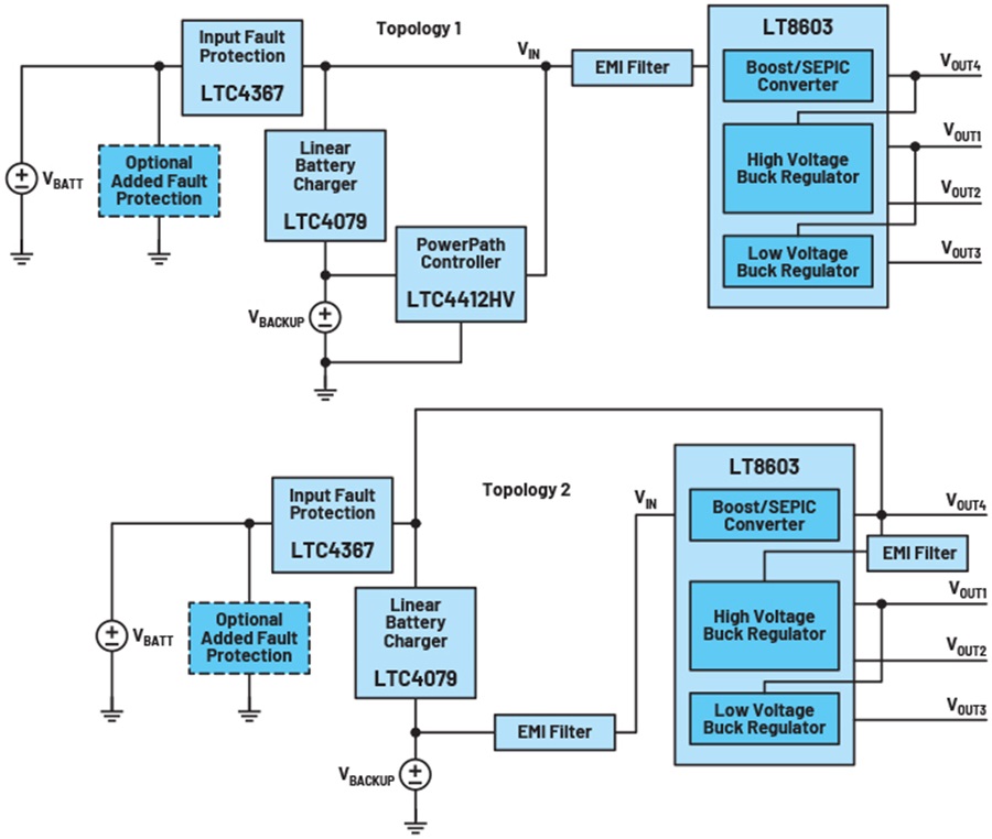
The flexibility of the schematic design allows variations on how the circuitry can be implemented. The reference design board has “Do Not Install” components and path connectors that allow the user to configure the board with either Topology 1 or Topology 2. This also allows the configuration of either a boost or SEPIC converter on VOUT4 depending on the application. An additional circuit option for added input fault protection can be implemented on the LTC4367 for 150 V transient conditions. More details on the configuration are shown on the schematic of the reference design board.
The circuit configuration presented in Figure 5 is Topology 1, which has a minimum VBACKUP voltage of 2.5 V, one EMI filter after VIN, and is capable of power switch-over through the LTC4412HV. The VIN of the boost controller sources its power from VBATT or VBACKUP. During the VBATT valid window, VOUT4 maintains a regulated voltage level through the boost converter or follows VBATT as shown in Figure 6. Outside the VBATT valid window, VOUT4 sources from VBACKUP in order to maintain a regulated set level.
Topology 2 addresses the need for a lower VBACKUP voltage application such as a 1.5 V level. When there is no input fault, VBATT is directly connected to VOUT4 while VBACKUP is the VIN to the boost controller. Additional filters are required on the input of the buck regulators for better noise filtering and EMI performance. Power switch-over is achieved seamlessly when VBATT falls below or goes above its valid window. The minimum VBATT voltage level of the valid window is set to the regulated level of VOUT4. During the VBATT valid window, VOUT4 follows VBATT. Outside of the VBATT valid window, VBACKUP is used to maintain a regulated set level.

Figure 11. Circuit variations.
| Topology 1 | Topology 2 | |
| ICs Used | LT8603, LTC4412HV, LTC4367, LTC4079 | LT8603, LTC4367, LTC4079 |
| Backup Battery Operation | VBACKUP operates as low as 2.5 V | VBACKUP operates as low as 1.5 V |
| EMI Input Filtering | Connected before boost regulator | Connected before boost and buck regulators input |
| Minimum VBATT Valid Window | VBATT can go as low as the VBACKUP level | VBATT must be equal to VOUT4 regulated set level |
Conclusion
The ever-growing advancement of automotive applications requires more reliability and safety considerations. The standards defined by international organizations have played a significant role for designers focusing on what contributes to the voltage transients that may be harmful or can cause degradation of the electronic system. In conclusion, the quad output power reference design has proven its capability when exposed to the simulated test conditions of input overvoltage, undervoltage, and reverse voltage operations. Also, the different circuit variations allow flexibility with regards to the backup battery operation, minimum battery voltage level, EMI input filtering, and the number of components. For more information about the reference design board, contact the authors or your local ADI representative.
Reference Design ICs and Files
Attached here are the schematic, PCB Gerber files, and the bill of materials (Topology 1) of the quad output regulator. For evaluation board availability, contact the authors or your local ADI representative.
References
Eddleman, Dan. “Low Quiescent Current Surge Stopper: Robust Automotive Supply Protection for ISO 7637-2 and ISO 16750-2 Compliance.” Analog Devices, Inc., January 2017.
Eddleman, Dan. “LTspice: Models of ISO 7637-2 & ISO 16750-2 Transients.” Analog Devices, Inc.
ISO 16750-2:2012: Road Vehicles—Environmental Conditions and Testing for Electrical and Electronic Equipment—Part 2: Electrical Loads. International Organization for Standardization, November 2012.
Wu, Bin and Zhongming Ye. “Comprehensive Power Supply System Designs for Harsh Automotive Environments Consume Minimal Space, Preserve Battery Charge, Feature Low EMI.” Analog Dialogue, Vol. 53, No. 3, August 2019.


