- Abstract
- Current Challenges in Power Stage Design
- Isolated DC/DC Converters for IGBTs, Si, and SiC MOSFETs
- RxxC2Txx Series: Reliable Performance for High-Power Applications (Download/Login)
- Key Applications (Download/Login)
- Conclusion (Download/Login)
Abstract
As industries transition to higher switching frequencies and voltages to improve performance and minimize overall system size, designers are finding it increasingly challenging to balance cost, efficiency, and reliability. A critical aspect of power stage design optimization is selecting appropriate gate drive solutions that can adapt to the always-changing current and emerging transistor technology requirements — such as silicon (Si), silicon carbide (SiC), and gallium nitride (GaN). This paper explores the challenges associated with standard gate drive designs and highlights the benefits of using isolated DC/DC converters with programmable outputs to achieve efficient, flexible, and future-proof gate drive power for IGBTs, Si, and SiC MOSFETs.
Current Challenges in Power Stage Design
Power conversion system designers face a dilemma when selecting gate drive solutions for their power stages — fixed gate drive voltage solutions, while simple to implement, lack the flexibility to accommodate different transistor technology requirements. For instance, optimal gate voltages for IGBTs, Si and SiC MOSFETs vary, consequently requiring the use of gate drive circuits or a total power stage redesign for newer transistor generations.
IGBTs typically require a positive gate voltage between +15V and +20V to fully turn on. For rapid turn-off and false triggering prevention, IGBTs require a negative gate voltage between -5V and -15V. Si MOSFETs have lower gate voltage requirements in contrast, generally needing between +10V and +15V to turn on and between 0V and -5V to turn off. SiC MOSFETs, chosen for their high switching speeds and low on-state resistance, have gate voltages close to those of IGBTs — with some devices requiring up to +25V for optimal performance. Using fixed gate drive voltage solutions for multiple transistors can lead to suboptimal performance, increased loss, and failure due to insufficient or excessive gate voltages. Designers may consequently resort to using separate gate drive circuits tailored to each transistor type, which increases not only the overall system complexity, but also cost and board space.
Increasing the switching frequency and voltage to enhance both efficiency and power density introduces certain challenges. Higher frequencies require faster switching transitions, which can result in increased EMI and noise issues. Faster switching edges (high dv/dt and di/dt) can couple noise through the circuit’s parasitic capacitances, including the transistor package, PCB traces, and isolation barriers. This noise interferes with the gate drive circuit’s proper operation, leading to unintended switching and even increased power loss and device failure.
Using high-performance components to achieve faster switching comes at a premium, as designers must strike a balance between cost and performance based on the application and market requirements. For example, designers may opt for lower-cost Si MOSFETs or IGBTs in cost-sensitive consumer applications. This decision sacrifices efficiency and performance in favor of a cheaper solution. On the other hand, in high-performance industrial or automotive applications, using expensive SiC MOSFETs may be justified to achieve efficiency, reliability, and power density benchmarks.
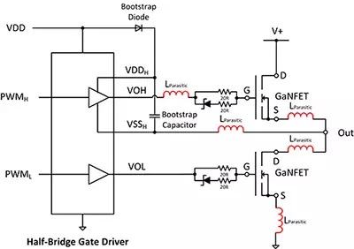
The need to reduce overall system size is another significant challenge in power stage design. As power density becomes increasingly important, designers must find ways to achieve greater miniaturization and seamlessly integrate gate drive circuitry without compromising performance or reliability. Unfortunately, standard gate drive solutions rely on discrete components and separate power supplies, which can occupy valuable board space and complicate the design. Discrete gate drive circuits consist of the following: a gate drive IC, isolated power supply, passive components such as resistors, capacitors, diodes, and more. Carefully selecting and placing each component on the PCB can only be done after considering factors such as power dissipation, thermal management, and signal integrity. As the number of transistors in a power stage increases, so does gate drive circuitry complexity and size.
Isolated DC/DC Converters for IGBTs, Si, and SiC MOSFETs
Most isolated DC/DC converters available on the market come with fixed output voltages. This lack of flexibility makes it difficult to accommodate the gate voltage requirements of different transistor technologies, including IGBTs, Si, and SiC MOSFETs. As a result, designers may need to use multiple isolated DC/DC converters or resort to additional circuitry to achieve the required gate drive voltages, which increases system complexity, size, and cost.
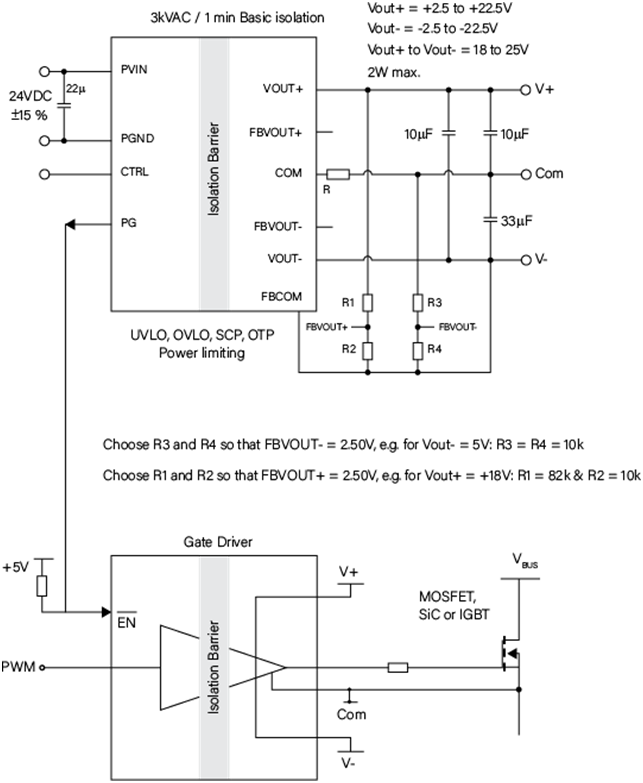
To address this problem, designers are turning to programmable isolated DC/DC converters as a solution. These converters combine the functionality of an isolated power supply and a gate drive circuit into a single package, while offering the ability to adjust the output voltages to match the needs of the chosen transistor technology. By providing gate drivers with programmable output voltages for each transistor, designers can optimize turn-on and turn-off characteristics of their power stage while simplifying the overall design and reducing system size.
Using programmable isolated DC/DC converters offers the ability to independently control the positive (Vpos) and negative (Vneg) gate voltages for individual transistors. This flexibility allows designers to fine-tune gate drive voltages, ensuring full enhancement and rapid discharge of the transistor while minimizing switching losses and improving efficiency. By selecting specific Vpos and Vneg values, gate voltages can be kept within a transistor’s safe limits while maximizing the performance. For example, in an IGBT-based power stage, a programmable isolated DC/DC converter can be set to provide a Vpos of +15V and a Vneg of -8V, ensuring full enhancement during turn on and rapid gate capacitance discharge during turn-off. Similarly, in a SiC MOSFET design, the converter can be configured to offer a Vpos of +20V and a Vneg of -5V, optimizing the gate drive voltages for the specific requirements of the SiC device.


In high-power systems, fast-switching transistors generate considerable common-mode transients, which can couple through the isolation barrier and disrupt gate drive signals. A high rating CMTI ensures that a converter maintains signal integrity and reliable operation even in the presence of these transients. The R24C2T25 also features an ultra-low isolation capacitance of less than 3.5pF, crucial for minimizing common-mode noise and reducing the impact of high dv/dt transients on the gate drive signals. In high-power applications, the switching transistors can generate large.

- Short circuit protection: In the event of an output short circuit, the R24C2T25 will detect the overcurrent condition and shut down the output to prevent damage to the converter and the connected circuitry.
- Overload protection: If the output current exceeds the converter’s rated current limit, the overload protection circuit will activate, reducing the output voltage to limit the current and protect the converter from damage.
- Overtemperature protection: The R24C2T25 includes an internal temperature sensor that monitors the converter’s temperature. If the temperature exceeds a safe threshold, the overtemperature protection circuit will trigger, shutting down the output to prevent converter thermal damage.
- Undervoltage lockout (UVLO): The R24C2T25 features both input and output UVLO protection. The input UVLO circuit monitors the input voltage and disables the output if the input voltage falls below a preset threshold preventing the converter from operating in an undervoltage condition, which could lead to unstable operation or damage to the connected circuitry. Additionally, the R24C2T25 incorporates an output UVLO circuit that monitors the output voltages. If the output voltages fall below a predetermined threshold, the output UVLO circuit will disable the output, preventing the converter from operating in output undervoltage conditions. This feature ensures that the gate drive circuitry receives a stable and reliable power supply, even if the output voltages deviate from their nominal values due to load variations or other factors.
- Power Good (PG) function: The R24C2T25 provides a Power Good output signal that indicates the converter’s output voltage status. This signal can be used to enable the gate drive circuit only when the output voltages are within the desired range.
KEY APPLICATIONS
The RxxC2Txx is suitable for a wide range of industries and systems where efficient, reliable, and flexible gate drive power is critical. Some key applications include:
Electric Vehicle (EV) Traction Inverters
In a typical EV traction inverter, high-power IGBTs or SiC MOSFETs convert the battery pack’s DC voltage into three-phase AC voltage for the traction motor. Efficiently driving these transistors is necessary to reduce switching losses and maximize the overall system efficiency. RECOM’s RxxC2Txx series is suitable for powering these gate drive circuits due to its programmable outputs and high isolation ratings. Designers can optimize the gate drive voltages for their SiC/IGBT power modules to achieve high efficiency and reliable operation under demanding EV application conditions.
The RxxC2Txx’s compact size and surface-mount package allows designers to create space-saving gate drive circuits for easy integration into the traction inverter’s PCB layout. This is particularly beneficial in EV applications where space is at a premium and minimizing the size and weight of electronic components is vital. High isolation ratings and low isolation capacitance of the RxxC2Txx also provide the necessary isolation and noise immunity. This isolation protects the low-voltage control circuitry from the higher voltages present in the EV inverter, while the low isolation capacitance minimizes high-frequency noise coupling and transients between the power and control circuits.


