Learn how to start working with PCBs in your lab or workshop.
- PCBs – how are they manufactured?
- Preparing the working space for PCB handling
- PBC preparation – workplace
- Working with printed-circuit boards – how to equip your workshop table?
- Hot air stations
- Work with PCB – first steps
- Preparing PCBs from scratch
- Soldering ready-made PCBs
- Tools and chemicals useful while handling printed circuits
Printed-circuit boards (PCB) can be found in each electronic device. They accommodate all necessary elements. They are connected via copper tracks protected from external conditions (such as oxidation) by a “solder mask”. Printed-circuit boards can be made of various materials, although the most commonly used solution is the PCB laminate comprising fibreglass and cured with epoxy resin. Such boards can be cut to various shapes and sizes.
PCBs – how are they manufactured?
There is a variety of processes for manufacturing printed circuit boards– from fully automated production lines manufacturing thousands of PCBs daily, to small workshops where individual PCBs are produced. Circuits are also commonly designed and etched at home by avid hobbyists and electronics enthusiasts. Electronic equipment breaks down occasionally. Sometimes, it is sufficient to replace a single PCB component, but, in some cases, we have to work a little harder.
This article covers a vast topic, i.e. how to prepare a workstation, equipment, as well as a PCB itself, to perform necessary work. It does not deal with professional production processes, focusing rather on working with PCBs in small workshops and at home.
Preparing working space for PCB handling
Before starting any work, it is a good idea to prepare suitable working space. While working at home, we do not really have much room to manoeuvre. The workshop must be located in a room, garage or basement. It is worth ensuring constant temperature and humidity in the room. Additionally, the floor should demonstrate ESD properties or (at least) be resistant to contact with corrosive substances.
PBC preparation – workplace
Undoubtedly, handling PCBs requires a suitable workstation. It is a good idea to have a desk or a professional workbench. Moreover, for safety reasons, they should be earthed. While organising a workstation, remember about storage space – e.g. additional drawers, as well as appropriate illumination. Here, we can use lamps dedicated to such purposes, but if the workstation has an additional shelf located above the working area, we can also install an additional strip of LEDs under it, which will significantly improve the lighting conditions.
Working with printed circuits also requires an ergonomic chair. On the market, there are workshop chairs available, whose surfaces are profiled ergonomically, thanks to which the work is not so tiring and, most importantly, we will avoid back problems in the future.
Working with printed-circuit boards – how to equip your workshop table?
If a workstation is ready to go, it is worth equipping it properly.
The first piece of equipment that comes to mind while designing an electronic workshop is, obviously a soldering iron. It is undoubtedly the most important device in a workshop. The best choice is a soldering station with temperature adjustment. The soldering iron power is also a factor that is worth paying attention to. In a nutshell: the higher the power rating, the faster the soldering tip reaches the desired temperature. It is particularly useful when soldering pads connected to fairly large ground areas.

WEL.WT1010HSET soldering station
Each soldering iron must come with a set of soldering tips suitable for various applications. For soldering SMD components, precision tips will prove most useful – conical or bevelled on one side. In this case, a small size of the tip allows to heat up a given soldering pad precisely. When working with surface-mounted ICs, a “mini-wave” tip will also be useful. It enables you to easily, even with one stroke of the tip, solder all the IC terminals on one side. Obviously, there are also slightly larger soldering tips available on the market, dedicated to soldering and desoldering of elements requiring heating up a much larger surface.

WEL.51303199 soldering tip regenerators
An important thing is that each soldering tip requires proper maintenance to significantly extend its life. The most common way to ensue maintenance of a soldering tip is to use dedicated metal-chip cleaners or special sponges soaked in water. In addition, chemical preparations for tip regeneration are also worth looking into.
Soldering mats placed on the workbench top are also worth recommending. Sometimes they come with small compartments, making it much easier to keep order while soldering and desoldering circuits.
Hot air stations
Another element important in the soldering or desoldering process is a hot air station. It is useful not only for mounting and desoldering small surface mount components (SMT), but also for heat-shrink tubing shrinking.

ST-862D hot air station

3M-5413-19 high-temperature tape
While discussing hot air stations, it is worth mentioning kapton tape, which, thanks to its resistance to high temperatures, protects certain components that we would not necessarily want to desolder. This tape is particularly useful when working with small PCBs on which most of the elements are made in SMD technology. Most often, we use it to cover the area around a soldered element, so the elements placed under the tape do not get moved or desoldered accidentally.
In the above-mentioned desoldering process which we can apply to remove any component from a PCB, such elements as a tin suction extractor and desoldering tape, commonly known as “braid”, are useful. They facilitate easy removal of excess tin from the soldering pad, which makes it easier to disassemble an electronic component. Each genuinely professional workshop must come with a desoldering station. It should be remembered, however, that such a station requires regular cleaning.

ERSA-VACX tin suction extractor
If you are going to work with PCBs on which surface-mounted circuits are placed, you should think about buying a professional BGA station. In addition to directional element heating, a BGA station also heats them from the bottom. In this way, we avoid stresses induced by temperature differences. Pre-heaters used together with stations will also be useful, as they help reduce surface tension.

AX-8450A table-mounted multimeter
Measurement and control equipment is also a useful part of any electronics workshop. Multimeters, oscilloscopes or logic testers can help us diagnose possible faults on a PCB.
In order to create your own printed-circuit board, one more device can be useful, namely a mini drill. If you are going to install certain elements on your PCB (THT assembly), you have to make appropriate holes in it. Their diameter is usually very small and, in addition, they are sometimes placed quite densely, so you need a precise device. Mini drills also require a set of small, precise drills.

PG-142MD mini drill
Work with a PCB – first steps
If our workshop is already equipped with basic equipment, we can now handle a PCB itself. Certain steps must be taken, depending on whether you just want to solder a ready-made board or prepare it from scratch.
Preparing PCBs from scratch
We have to somehow place all the tracks and solder fields on clean PCB laminate. The PCB etching process is used for this purpose. It consists in applying a protective layer so that the underlying copper layer is not degraded. There are many ways to etch PCB tracks, and the easiest one is to draw them with a marker or print a track image on chalk paper and transfer it on a PCB.
After applying the tracks, you can proceed with the etching process. To this end, place the board in a special solution of B327 or ferric chloride. This substance will remove copper in places where tracks have not been designed.
When the circuit is ready, it should be properly protected. For this purpose, the PCB undergoes the tin plating process, i.e. a layer of tin is applied on a layer of copper. This can be done manually or with the use of ready-made chemical preparations.
At the very end, covering the designed board with a solder mask is a sensible solution. It is an electrically inert chemical layer, which, apart from protecting the circuit against oxidation, also protects it against accidental short circuits.
Soldering ready-made PCBs

WEL.ESF120ESD PCB rig
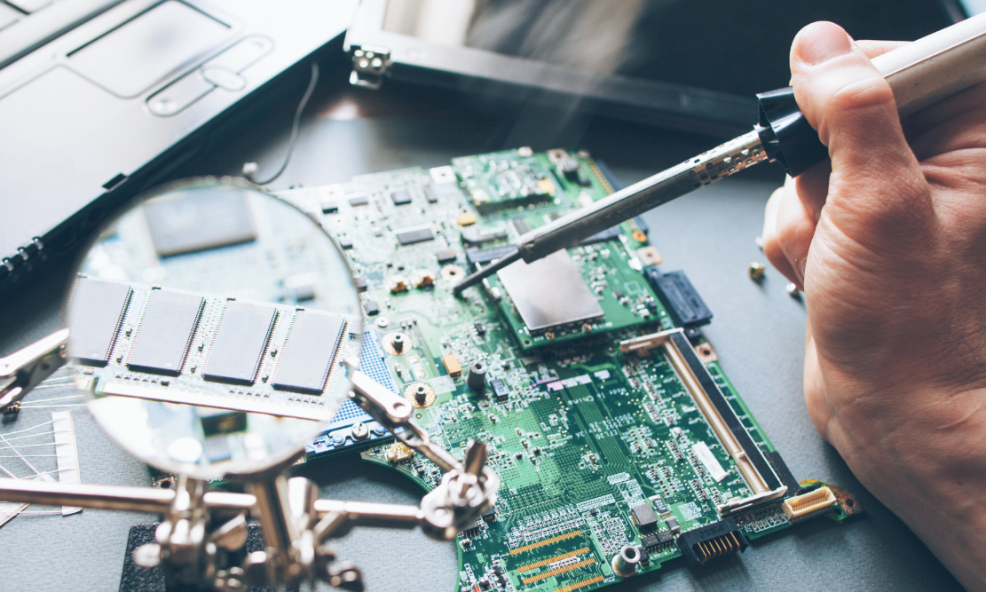
To facilitate the entire process, a PCB should be mounted in a special rig. It comes in numerous varieties, but the most common one is the “third-hand” rig equipped with a magnifying glass.
When a printed circuit is already stabilised, we can begin the soldering process. For this purpose, a soldering filler is indispensable. There are two types of soldering fillers available on the market, i.e. with or without lead content. The former is used less and less often, due to the harmful lead content, mainly in medical or military applications where reliability is of key importance. Lead-free solder is slightly more difficult to handle, but it does not emit hazardous fumes.
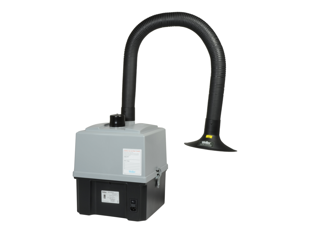
During the soldering process, harmful volatile substances are generated. Thus, it is worth investing in a fume extractor. It prevents fumes from entering our respiratory system, as they are extracted to the outside. They come in three different designs: standing on the desk, mounted on a movable arm and as a box with a pipe that can be mounted anywhere.

WEL.ZEROSMOGEL-KIT fume absorbers
Various fluxing agents are also useful in the soldering process. They greatly facilitate the soldering process, especially in the case of SMD components.
When a PCB is already soldered, it is most probably covered with flux residues or other deposits which must be removed. For this purpose, we can use the most common isopropyl alcohol (IPY) or dedicated spray cleaners. Such products often come with nozzles terminated with a brush to facilitate printed circuit cleaning. PCBs can also be cleaned with an ultrasonic cleaner requiring dedicated cleaning agents to this end. It is also worth paying attention to no-clean fluxes which, thanks to their composition, do not require any cleaning.
After cleaning and drying, a PCB can be coated with a special layer of PCB varnish to protect it against undesirable impact of external conditions. Gels and pastes can also be used to protect PCBs. It is especially useful when a device is operated outdoors or in unfavourable production conditions. A PCB prepared in this manner can be considered as fully finished and capable of operating in a device enclosure.
Tools and chemicals useful while handling printed circuits
When working with PCBs, precision tweezers may come in handy. We can use them both while soldering and desoldering a given circuit. “Sharp-tipped” tweezers are most useful to adjust and fit an element within a soldering field.
Most PCBs are placed in various types of devices whose enclosures need to be opened. For this purpose, tools such as screwdrivers with different tips, pliers or clippers are useful, i.e. items that usually are part of standard equipment of an electronic workshop. As mentioned above, various chemicals can also be used to handle PCBs, e.g.: isopropyl alcohol, fluxes and tip regenerating substances or PCB varnish. In addition, the following might also come in handy: rosin, which, similarly to flux, facilitates the soldering process, spray / liquid “contact” for e.g. potentiometer regeneration, or thermally conductive adhesives to attach a heat sink.
In summary, the subject of workshop equipment and wok with PCBs is truly extensive. We must design a suitable workstation and equip it with tools and materials that will enable us to work accurately and safely. Following such preparations, we can easily start working with PCBs.
Text prepared by Transfer Multisort Elektronik Sp. z o.o.
The original source of text: tme.eu


